SEM sample metallizer
SPT-20
1. Easy to use
2. Digital interface
3. Adaptation to each samples
Non-conductive samples often have a charge effect due to the accumulation of electrons on the surface, which poses problems for collecting a good image. Although SEM's "low vacuum" or "load reduction" mode can overcome this problem, this mode generally has limitations in terms of magnification and image quality depending on the sample.
To obtain the best possible image quality, the non-conductive samples are generally covered using a sputtering device which applies a nanometric layer of conductive metal. This coating allows imaging at higher beam energies to achieve the highest resolution and magnification without worrying about the effects of electronic charge or beam damage to sensitive samples.
Non-conductive samples can often be imaged under high vacuum using a low beam energy of 1 to 5 kV using the SE detector, with possible magnification limitations. Although non-conductive samples can be imaged in low vacuum mode, a sputtering device is a valuable tool for electron microscopy, which provides the largest magnifications and better quality images.
EDS analysis can always be performed on coated samples, since most EDS software allows the coating metal to be defined so that it is not taken into account during the analysis. A type of metallic coating is selected which is not present in the sample. Alternatively, a layer of carbon can be used to produce an X-ray transparent conductive coating. This is popular in the mineralogical analysis of polished resin-mounted samples. Please contact us to discuss purchasing a Carbon Coater for EDS, as other solutions may work for your sample types before investing in a dedicated carbon coater.
Scanning electron microscopy
MEB optional metallizer
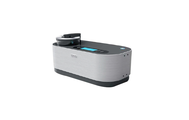
SPT-20
The Coxem SPT-20 metallizer offers great ease of use via its digital interface allowing the parameters to be adapted to each of your samples.
- Digital ion metallizer
- Easy to use (Choice of coating, current, vacuuming via a single system)
- Stable metallization via "Coating Current Feedback" mode
- Works with several types of target
- Rotary pump with low noise level
- Target: Au, Pt, Cu, Cr,…
- Target size: 50 mm
- Ionization current: 0 - 9 mA
- Chamber size: 100 mm
- Dimensions: 420 (L) * 220 (W) * 230 (H) mm
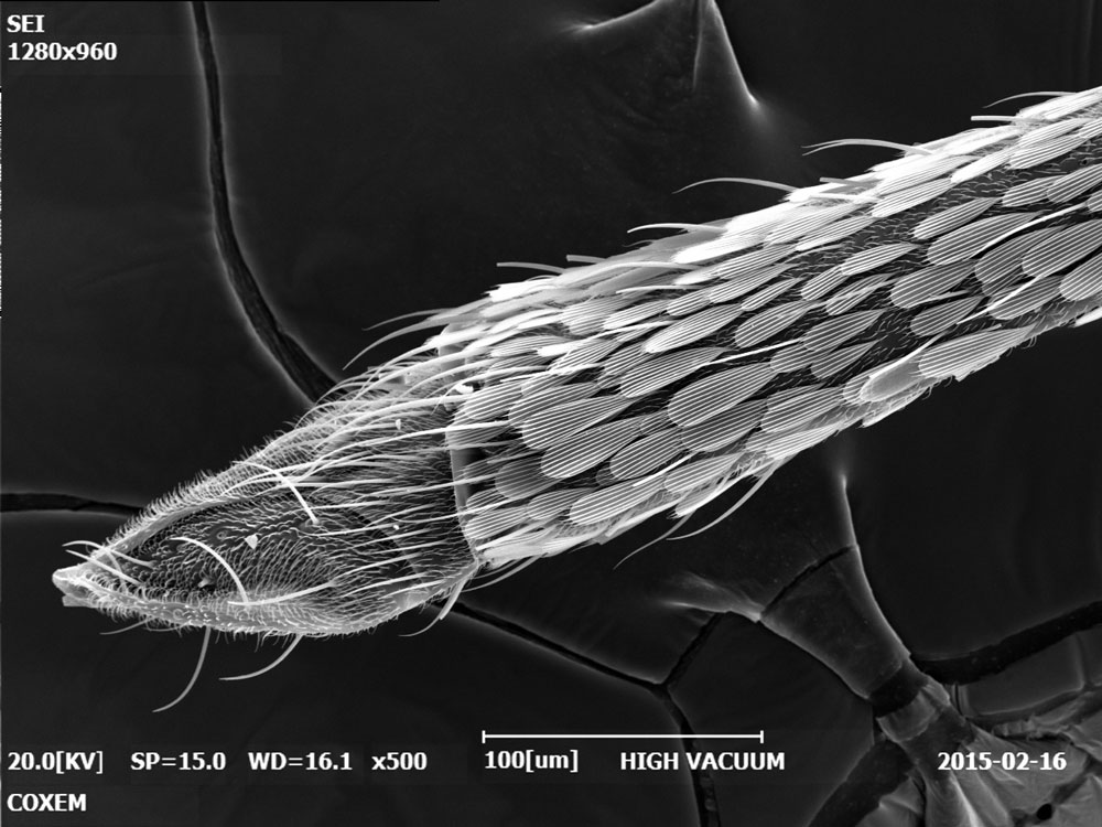
Mosquito stinger
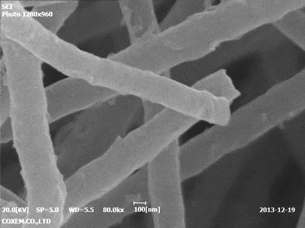
Nanotubes 80000x
Silicon wafer 2
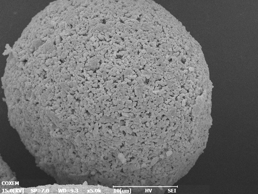
X2-5
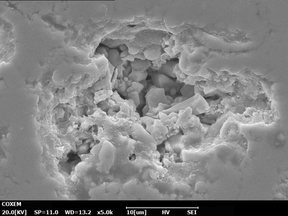
3-4
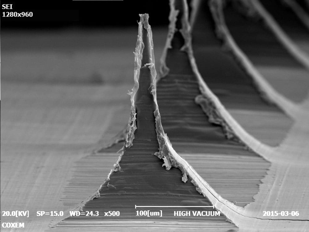
Cosmetic patch
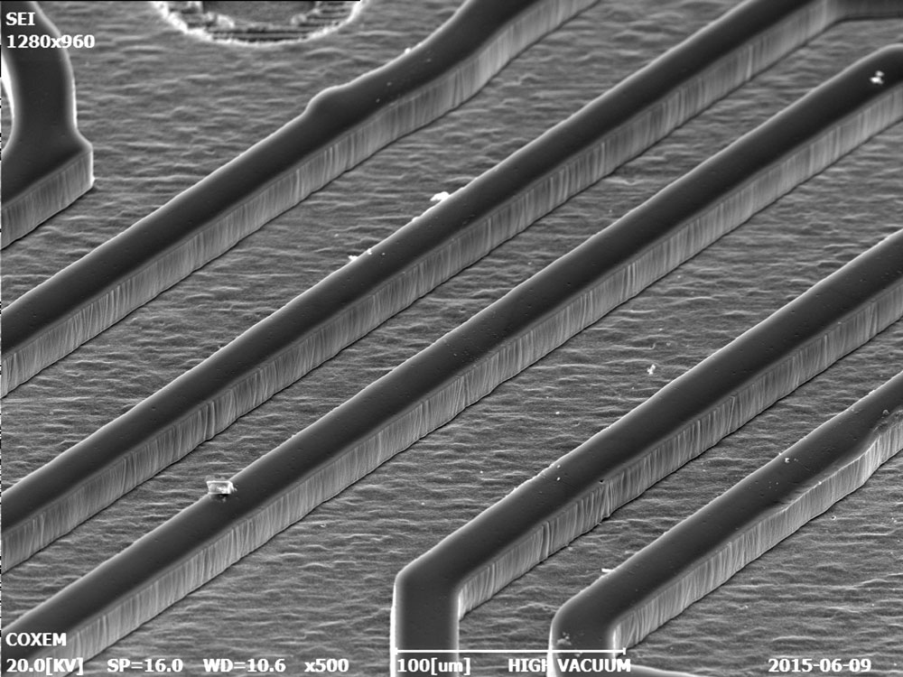
Etch-500x
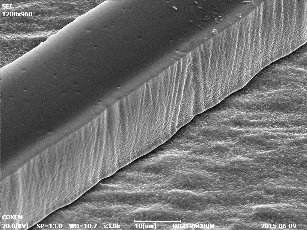
Etch-3000x
Contact us for more information on this product
Would you like an estimatation ?
Additional information?
We will reply to you within 24 hours


