Automated thin-film thickness mapping
F54
1. Sample up to 450 mm in diameter
2. No limit on the number of points
3. Easy to use
4. Wide wavelength range
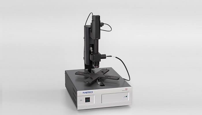
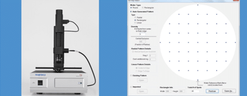
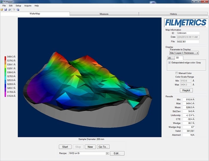
Thin-film thickness of samples up to 450 mm in diameter are mapped quickly and easily with the F54 advanced spectral reflectance system. The motorized r-theta stage moves automatically to selected measurement points and provides thickness measurements as fast as two points per second.
- F50 Serie : Customizable thickness mapping - best cost/effective solution. More information >
- F54-XY-200mm Serie : Acoustic protection cover - Production. More information >
- F60 Serie : High automation - notch detection - SECS / GEM interface. More information >
Applications
-
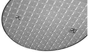
FABRICATION SEMI-CONDUCTEUR
-
Photorésist
-
Oxydes / Nitrures / SOI
-
Rectification / emballage de wafer
AFFICHAGES EN CRISTAL LIQUIDE
- Lacunes cellulaires
- Polyimide
- ITO
REVÊTEMENTS OPTIQUES
- Revêtements de dureté
- Revêtement antireflet
- Filtres
MEMS
- Photorésist
- Membranes de silicium
- Filtres de couche mince AlN / ZnO
-
More info on applications
- Dielectric
- Hard thickness
- IC failure analysis
- ITO and other TCO
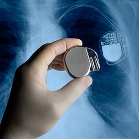
- Medical equipement
- Metal thickness
- Microfluidics
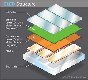
- OLED
- Ophthalmic coatings
- Parylene Coatings
- Photoresist
- Porous silicon
- Treatment films
- Refractive index & k
- Wafers and membranes of silicon
- Solar applications
- Semiconductor teaching laboratories
- Roughness and surface finish
Automated Thin-Film Thickness Mapping System
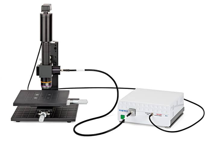
Choose one of the dozens of predefined polar, rectangular, or linear map patterns, or create your own with no limit on the number of measurement points. The entire desktop system is set up in minutes and can be used by anyone with basic computer skills.
The F54 film thickness mapping system connects to the USB port of your Windows® computer and can be set up in minutes.
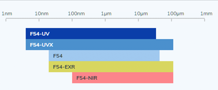
The different instruments are distinguished primarily by thickness and wavelength range. Generally shorter wavelengths (e.g. F54-UV) are required for measurement of thinner films, while longer wavelengths allow measurement of thicker, rougher, and more opaque films.
ADVANTAGES
- Sample up to 450 mm in diameter
- No limit on the number of points
- Easy to use
- Wide wavelength range
Accessories
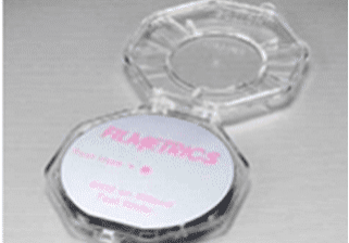
NIST-traceable thickness standard
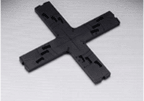
F50 chuck - 100mm, 200mm, 300mm & 450mm
Specifications
Model Specifications
| Model | Thickness Range* | Wavelength Range |
|---|---|---|
| F54 | 20nm - 45µm | 380-1050nm |
| F54-UV | 4nm - 35µm | 190-1100nm |
| F54-NIR | 100nm - 115µm | 950-1700nm |
| F54-EXR | 20nm - 115µm | 380-1700nm |
| F54-UVX | 4nm - 115µm | 190-1700nm |
*film stack dependent
Thickness Range*
Contact us for more information on this product
Would you like an estimation ?
Additional information?
We will reply to you within 24 hours


