Automated thin-film thickness mapping
F60
1. Dedicated to production
2. Automated
3. Fast
4. Customizable
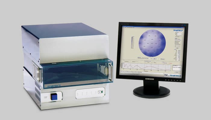
The F60-t family maps film thickness and index just like our F50 products, but it also includes a number of features intended specifically for production environments. These include automatic notch finding, automatic on-board baselining, an enclosed measurement stage with motion interlock, and an industrial computer with pre-installed software.
- F50 Serie : Customizable thickness mapping - best cost/effective solution. More information >
- F54 Serie: Fine spot size - sample up to 450mm in diameter - R&D. More information >
- F54-XY-200mm Serie: Acoustic protection cover - Production. More information >
Applications
-
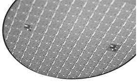
SEMICONDUCTOR FABRICATION
-
Photorésist
-
Oxides
-
Nitride
-
Polysilicon
LIQUID CRYSTAL DISPLAYS
- Cell Gaps
- Polyimide
OPTICAL COATINGS
- Hardness Coatings
- Anti-Reflection Coating
- Filters
-

More info on applications
- Dielectric
- Hard thickness
- IC failure analysis
- ITO and other TCO
- Medical equipement
- Metal thickness
- Microfluidics
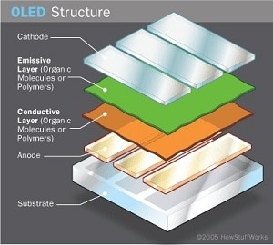
- OLED
- Ophthalmic coatings
- Parylene Coatings
- Photoresist
- Porous silicon
- Treatment films
- Refractive index & k
- Wafers and membranes of silicon
- Solar applications
- Semiconductor teaching laboratories
- Roughness and surface finish
Automated Thickess Mapping for Production Environments
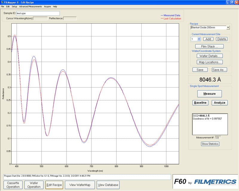
Thin-film thickness and n & k are mapped quickly and easily with the F60 advanced spectral reflectance system. The motorized R-Theta stage moves automatically to selected measurement points and provides thickness measurements in seconds. Choose one of the dozens of predefined polar, rectangular, or linear map patterns, or create your own with no limit on the number of measurement points. A typical 49-point map takes about 45 seconds.
Included are a number of features intended specifically for production environments, such as automatic notch finding, automatic on-board baselining, an enclosed measurement stage with motion interlock, and an industrial computer with pre-installed software.
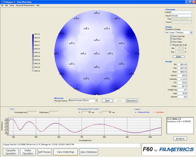
ADVANTAGES
- Dedicated to production
- Automated
- Fast
- Customizable
Accessories
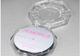
NIST-traceable thickness standard
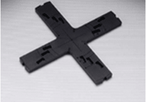
F50 chuck - 100mm, 200mm, 300mm & 450mm
Specifications
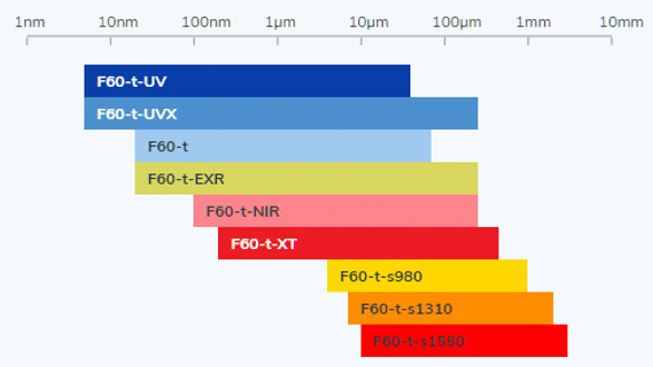
Model Specifications
| Model | Thickness Range* | Wavelength Range |
|---|---|---|
| F60-t | 20nm - 70µm | 380-1050nm |
| F60-t-UV | 5nm - 40µm | 190-1100nm |
| F60-t-NIR | 100nm - 250µm | 950-1700nm |
| F60-t-EXR | 20nm - 250µm | 380-1700nm |
| F60-t-UVX | 5nm - 250µm | 190-1700nm |
| F60-t-XT | 0.2µm - 450µm | 1440-1690nm |
| F60-s980 | 4µm - 1mm | 960-1000nm |
| F60-t-s1310 | 7µm - 2mm | 1280-1340nm |
| F60-t-s1550 | 10µm - 3mm | 1520-1580nm |
*film stack dependent
Thickness Range*
Contact us for more information on this product
Would you like an estimation ?
Additional information?
We will reply to you within 24 hours


